Lepower Shares: High-power LED light source packaging technology and structural form analysis
2016-09-27
With the rapid increase in the penetration rate of LED commercial lighting and home lighting, market demand continues to grow. The form of packaging also began to gradually move toward formalization. At present, the mainstream packaging methods of LED in the lighting market are mainly composed of small and medium-sized power products in PPA or PCT packaging, medium and high power LED in EMC packaging and traditional ceramic packaging and COB packaging.
High-power LED packaging, as an important link in the industrial chain, is the core manufacturing technology to promote semiconductor lighting and display to practical use. Only through the development of low thermal resistance, high light efficiency and high reliability of LED packaging and manufacturing technology, good mechanical and electrical protection of LED chips, reduce the impact of mechanical, electrical, thermal, wet and other external factors on chip performance, ensure the stable and reliable work of LED chips, in order to provide efficient and sustained high-performance lighting and display effects. To achieve the unique advantages of energy saving and longevity of LED, and promote the sound development of the entire semiconductor lighting and display industry chain.
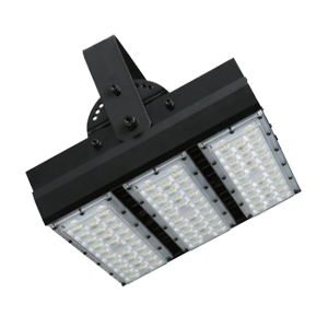
Packaging technology plays a crucial role in LED performance. The choice of LED packaging method, material, structure and process is mainly determined by the chip structure, photoelectric/mechanical characteristics, specific application and cost. With the increase of power, especially the needs of the development of solid-state lighting technology, new and higher requirements have been put forward for the optical, thermal, electrical and mechanical structures of LED packages. In order to effectively reduce the thermal resistance of the package and improve the efficiency of the light output, a new technical idea must be adopted to carry out the package design. From the perspective of process compatibility and reducing production costs, the LED package design should be carried out at the same time as the chip design, that is, the chip design should take into account the package structure and process. At present, the main development trends of power LED packaging structure are: miniaturization of size, minimization of device thermal resistance, plane-mounted, maximum junction temperature tolerance, and maximum single light flux; The goal is to improve luminous flux, luminous efficiency, reduce light decay, failure rate, improve consistency and reliability. For example, the current flip EMC series products FE35 of Liyang shares can reach a maximum power of 3W and a luminous flux of 400lm, achieving a small luminous surface with high lumen output. Specifically, the key technologies of high-power LED packaging mainly include: thermal dispersion technology, optical design technology, structural design technology, phosphor coating technology, eutectic welding technology.
1, heat dissipation technology
The temperature of the general LED node can not exceed 120 ° C, so the thermal radiation effect of the LED device is basically negligible, and heat conduction and convection are the main ways of LED heat dissipation. In the heat dissipation design, the heat conduction is considered first, because the heat is first conducted from the LED package module to the radiator. Therefore, the bonding material and substrate are the key links of LED heat dissipation technology.
The bonding material mainly includes three main ways: thermal conductive adhesive, conductive silver paste and alloy solder. Thermal conductivity glue is to add some high thermal conductivity filler inside the matrix, such as SiC, A1N, A12O3, SiO2, etc., to improve its thermal conductivity; Conductive silver paste is a composite material formed by adding silver powder to epoxy resin. The hardening temperature of the paste is generally lower than 200℃, and it has the advantages of good thermal conductivity and reliable bonding performance. However, the absorption of light by the silver paste is relatively large, resulting in a decrease in light efficiency.
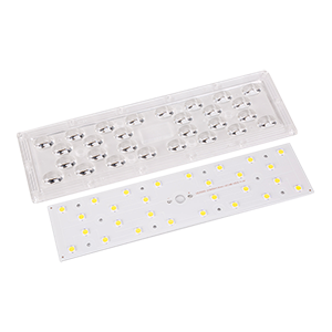
The substrate mainly includes ceramic substrate, metal composite substrate and composite substrate. The ceramic substrate is mainly LTCC substrate and AIN substrate. LTCC substrate has many advantages, such as easy molding, simple process, low cost and easy to be made into a variety of shapes. Al and Cu are excellent materials for LED packaging substrates, due to the electrical conductivity of metal materials, in order to insulate the surface, it is often necessary to pass anodizing treatment to form a thin insulating layer on the surface. Metal matrix composites mainly include Cu matrix composites and Al matrix composites. At present, the second generation COB products of Liyang Stock mainly use mirror aluminum substrate and copper substrate, such as 4046 mirror aluminum series light efficiency can reach 175lm/w.
In addition, the packaging interface has a great impact on the thermal resistance, the key to improve LED packaging is to reduce the interface and interface contact thermal resistance, enhance heat dissipation. Therefore, the selection of thermal interface materials between the chip and the cooling substrate is very important. Using low temperature or eutectic solder, solder paste or conductive adhesive doped with nanoparticles as thermal interface materials can greatly reduce the thermal resistance of the interface.
2. Optical design technology
The optical design of LED package includes inner optical design and outer optical design.
The key of internal optical design lies in the selection and application of potting adhesive. In the selection of potting adhesive, it is required to have high transmittance, high refractive index, good thermal stability, good fluidity and easy spraying. In order to improve the reliability of LED packaging, potting adhesives are also required to have the characteristics of low moisture absorption, low stress, temperature resistance and environmental protection. Currently commonly used potting adhesives include epoxy resin and silica gel. Among them, silica gel is widely used in high-power LED packaging because of its high light transmittance (transmittance greater than 99% in the visible light range), high refractive index (1.4 ~ 1.5), good thermal stability (can withstand 200℃ high temperature), low stress (Young's modulus is low), low moisture absorption (less than 0.2%), etc., which is obviously superior to epoxy resin.
External optical design refers to the convergence and shaping of the outgoing beam to form a uniform distribution of light intensity. It mainly includes the design of reflection condenser cup (primary optics) and shaping lens (secondary optics), and also includes the distribution of chip array for array module. The common shapes of the lens are convex lens, concave lens, spherical mirror, Fresnel lens, combined lens, etc. The assembly method of the lens and high-power LED can be air-tight package and semi-air-tight package. The patented moding technology can increase the light output rate by 10-15% at one time, and it is easy to distribute light twice.
3, LED package structure form
LED packaging technology and structure have been pin type, power type package, patch type (SMD), on-board chip directly mounted (COB) four stages.
(1) Pin type (Lamp)LED package
LED pin package using lead frame for a variety of package shape pin, is the first successfully developed package structure put on the market, a large number of varieties, high technical maturity, package structure and reflection layer is still improving. Commonly used 3 ~ 5mm package structure, generally used for small current (20 ~ 30mA), low power (less than 0.1W) LED package. Mainly used for instrument display or indication, large-scale integration can also be used as a display screen. The disadvantage is that the thermal resistance of the package is large (generally higher than 100K/W) and the life is short.
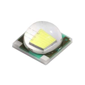
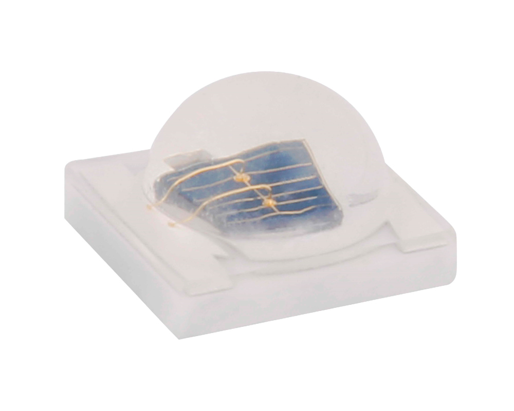
(2) Power LED package
LED chip and package to the direction of high power development, in the large current generation than Φ5mmLED 10 to 20 times the luminous flux, must use effective heat dissipation and non-deterioration of the packaging material to solve the problem of light decay, therefore, the shell and package is also the key technology, can withstand the number of W power LED package has appeared. 5W series white, green, blue green, blue power LED supply from the beginning of 2003, white LED light output up to 1871m, light efficiency 44.31 lm/W green light failure problem, developed can withstand 10W power LED, large area tube; The size is 2.5mm X2.5mm, can work at 5A current, light output up to 2001 lm, as a solid lighting source has a lot of room for development.
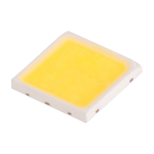
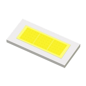
(3) Surface assembly (patch) type (SMD)LED package
As early as 2002, surface-mount packaging LED(SMDLED) gradually accepted by the market and gained a certain market share from pin-type packaging to SMD in line with the general trend of the development of the entire electronics industry, many manufacturers launched such products.
SMDLED is the current LED market share of the highest package structure, this LED package structure uses the injection molding process to wrap the metal lead frame in PPA plastic, and form a specific shape of the reflection cup, the metal lead frame extends from the bottom of the reflection cup to the side of the device, by outward flat or inward bending to form the device pin.
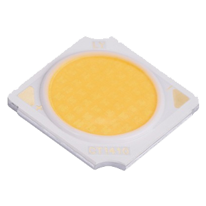
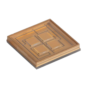
(4)COB-LED package
COB package can directly package a number of chips on a metal-based printed circuit board MCPCB, and direct heat dissipation through the substrate can not only reduce the manufacturing process and cost of the bracket, but also reduce the heat dissipation advantage of thermal resistance. The PCB board can be a low-cost FR-4 material (glass fiber reinforced epoxy resin), or it can be a metal or ceramic matrix composite material with high thermal conductivity (such as aluminum substrate or copper-coated ceramic substrate, etc.). The lead bonding can be performed by thermoultrasonic bonding at high temperature (gold ball welding) and ultrasonic bonding at normal temperature (aluminum splice welding). COB technology is mainly used for high-power multi-chip array LED package, compared with SMD, not only greatly improve the package power density, but also reduce the package thermal resistance (generally 6-12W/m稫).
From the point of view of cost and application, COB will become the mainstream direction of future lighting design. The COB package LED module is installed on the bottom plate of a number of LED chips, the use of multiple chips can not only improve the brightness, but also help to achieve a reasonable configuration of the LED chip, reduce the input current of a single LED chip to ensure high efficiency.
In short, whether it is a single-device package or a modular COB package, from small power to high power, the design of the LED package structure is centered on how to reduce the thermal resistance of the device, improve the light effect and improve reliability.
4, phosphor coating technology
The light conversion structure, that is, the phosphor coating structure, is mainly for LED white light lighting technology, which aims to convert the short wavelength light emitted by the LED chip into a longer wavelength light that is complementary to it (color complementary to form white light).
5, eutectic welding technology
Eutectic welding technology is one of the most important core technologies in the packaging process of high-power LED flip chip. The advantages of eutectic welding technology, which is the core heat dissipation problem and solid crystal problem in the LED packaging process, are and will become the mainstream direction of LED packaging development in the future. The melting point of eutectic alloy is lower than that of pure component, and the melting process is simple. Eutectic alloys have better fluidity than pure metals, which can prevent the formation of dendrites that hinder liquid flow during solidification, thus improving the casting performance. Eutectic alloys also have thermostatic transition characteristics (no solidification temperature range), which can reduce casting defects such as polarization and shrinkage; After curing, the eutectic alloy has strong toughness (close to the toughness of metal) and should not be broken. Eutectic solidification can obtain a variety of microstructure, especially the regular arrangement of layer or rod eutectic microstructure, which can become excellent in-situ composite materials. It is because eutectic has so many advantages that LED packages made using the eutectic process have the advantages of reducing impedance and improving heat transfer efficiency.